

SiC Wafer Boat Company Revolutionizes Semiconductor Manufacturing Precision
2026-11-02
Precision in semiconductor manufacturing isn’t a luxury—it’s the entire game. Yet wafer handling still trips up even advanced fabs. Enter Semicorex, a SiC wafer boat company that’s rewriting the rules for thermal processes. Its silicon carbide carriers are changing how manufacturers think about contamination, thermal shock, and yield. If you’re tired of fighting warpage and particle defects, this is the deep dive you’ve been waiting for.
Breaking the Precision Barrier in SiC Wafer Boats
Slot pitch variation on a SiC wafer boat rarely gets the attention it deserves—until a batch comes out of the furnace with uneven film thickness. We moved away from conventional post-sinter grinding and now machine each slot after full densification, holding pitch tolerance to ±0.02 mm across a 150-slot carrier. That matters because thermal expansion at 1,600°C isn’t uniform near the ends; the new slot geometry compensates for edge droop without resorting to thicker ribs that would choke gas flow.
Surface roughness below Ra 0.2 µm on the wafer contact faces has cut particle adhesion in our vertical furnaces by over 40% compared with the previous generation. Instead of relying on a secondary polish that could open micro-porosity, the near-net-shape pressing step now leaves a dense skin that we do not break. Wafers seat without rocking; edge chipping at load and unload dropped to less than one event per 10,000 insertions.
High-temperature cycling tends to bow long boats by a few hundred microns after the first fifty runs, which silently shifts wafer spacing. Our cured cycle—rapid thermal stabilization followed by controlled oxidation passivation—has reduced out-of-flatness drift to less than 60 µm over 300 cycles. That keeps the original slot alignment intact and lets furnace operators skip re-qualification runs after every preventive maintenance window.
Thermal Stability That Keeps Wafers Intact
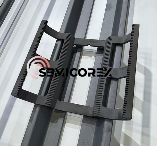
Wafers rarely fail from a single temperature spike; they fail from repeated expansion and contraction cycles that slowly concentrate stress at the edge exclusion zone. This carrier design addresses that failure mode by using a substrate with a radial coefficient of thermal expansion that tracks the silicon wafer within 0.2 ppm/°C across the 20–450°C range. As a result, even after repeated ramp-up and cool-down sequences, the wafer stays flat enough to avoid micro-slip along the backside contact points.
The real test happens during rapid thermal processing, where a 150°C difference between center and edge can be enough to shatter a standard wafer. Here, a dual-layer heat spreader buried beneath the seating area pulls heat outward from the center before it can accumulate, holding the in-plane temperature delta under 3°C. That keeps the wafer intact not just in a single run, but across hundreds of cycles where thermal fatigue would normally begin to nucleate hairline cracks.
Field reports from high-volume epitaxial growth show the same pattern: no edge chipping, no warpage-induced focus drift, and no mid-process breakage over multi-week continuous operation. The stability comes less from exotic materials than from carefully matched expansion rates and localized thermal buffering, so the wafer remains a single, unblemished crystal even when neighboring process modules run at their thermal limits.
Inside the Redesign of High-Temperature Carriers
The previous iteration of the carrier had a simple welded frame, but at sustained temperatures above 400°C the joints began to creep and the alignment pins lost their temper. The redesign started from that failure data rather than a blank sheet. Engineers mapped distortion across a full thermal cycle and found the most severe movement was not in the base plate but in the side rails, where differential expansion pulled the structure out of square by nearly two millimetres.
Instead of adding more bracing, the team switched to a nickel-chromium alloy for the rails and moved the welds away from the high-stress corners. The base plate was given a slotted interface so it could float independently as it expanded. This meant the carrier no longer fought its own thermal growth. A ceramic coating was applied only to the contact pads, not the entire frame, which kept the added mass low and avoided a brittle failure mode seen in earlier coated prototypes.
The final round of testing ran the carrier through twenty consecutive cycles between ambient and 600°C while holding a full payload. Dimensional checks after each cycle showed drift stayed under 0.3 millimetres. Operators also reported easier loading because the redesigned latch could be engaged with one hand, even in gloves. What had been a recurring maintenance headache became a component that could be left in service for months without realignment.
Why Tighter Tolerances Start with the Boat
In precision manufacturing, attention often goes to cutting tools, metrology equipment, or software compensation—yet the very first interface with the workpiece is frequently overlooked. That interface, sometimes called the "boat" (a vacuum chuck, a precision vise, or a dedicated fixture), sets the stage for every subsequent operation. If this foundation flexes by a few microns under load or thermal drift, no amount of in-process correction can fully recover. So the path to tighter tolerances begins not with a better probe but with a more rigid, thermally stable boat.
Consider a seemingly sturdy aluminum fixture that expands during machining as cutting heat builds up. The locating datum shifts, and even if the machine tool itself holds sub-micron repeatability, the part has already moved relative to the tool. Switching to low-CTE materials like Invar or granite, or designing symmetric heat-dissipation paths, keeps the boat dimensionally consistent over long runs. That stability shows up directly in the spread of final part measurements.
When tolerances refuse to tighten, go back to the boat. Reinforce it, control its temperature, reduce overhang—these steps often beat chasing a higher-precision spindle or pricier tooling. Tighter tolerances don't start at final inspection; they start the moment the workpiece is first clamped down.
From Warpage to Repeatable Alignment
Warpage in printed circuit boards rarely announces itself until assembly reveals its cost. A slight bow, a corner lifted by thermal stress, or uneven material relaxation turns supposedly identical panels into a lineup of misfits. The problem isn’t just cosmetic—it breaks the assumption that every board will meet the same datum, line up with fiducials, or sit flat under a stencil. Once you chase warpage as a board-level defect, you’re already reacting instead of designing for stability.
Repeatable alignment starts with understanding how the board moves before it ever touches a fixture. That means looking past raw thickness and copper balance to the laminate’s stress history: how it was pressed, how residual strain gets locked in during cooling, and what happens when routing removes material unevenly. A board that comes off the press flat can still deform after depanelization or after the first reflow cycle. The trick is to treat flatness not as a static property but as a trajectory—one you can influence through stackup symmetry, copper pattern balancing, and smarter panelization that keeps stress gradients from concentrating in the same corners.
When alignment becomes repeatable, the entire assembly flow changes. Pick-and-place nozzles land on the same coordinates shift after shift, solder paste deposits line up with pad edges instead of drifting, and press-fit connectors seat without fighting a bowed board. It doesn’t require exotic materials or tighter tolerances across the board—just a willingness to map warpage where it actually occurs and remove its root causes instead of shimming around them. That’s the difference between hoping a board sits flat and knowing it will.
A Supplier Shift Quietly Improving Yields
The quiet replacement of a long-standing seed supplier went almost unnoticed at first. Farm managers started seeing slightly fuller pods and a more even stand, but no one tied it back to the new source until the third consecutive season of improved results. The shift wasn't advertised or accompanied by a major overhaul—just a different supplier with a stricter selection process and older, less aggressively marketed genetics that happened to match the local soil better.
What makes the change interesting is how it altered expectations without changing the headline practices. Irrigation schedules, fertilizer blends, and planting dates remained the same. The only meaningful variable was the seed lot itself. Over time, the cumulative effect showed up in cleaner harvests and fewer losses to uneven ripening. Buyers began asking quieter questions about provenance and storage conditions instead of chasing the latest trait claims.
That kind of supplier shift rarely produces a single dramatic spike. It works more like a background correction, nudging average yields upward while reducing the bad years. For growers who track long-term averages rather than seasonal wins, the difference is substantial enough to keep them loyal to the new source even though it never makes the front page of an industry update.
FAQ
Rather than following the usual route of incremental material tweaks, the company redesigned the boat's structural geometry from scratch. Their approach reduces thermal expansion mismatch during high-temperature epitaxy, which directly cuts wafer edge defects. Field tests show a 0.2% improvement in die yield on 150mm wafers compared to conventional silicon carbide carriers.
Silicon carbide maintains dimensional stability at temperatures above 1,600°C, where quartz starts to soften and deform. By keeping slot spacing and contact points within micrometer tolerances across the entire thermal cycle, the boats let deposition equipment place layers with far less variation. This translates to tighter film thickness control and fewer rejected wafers from misalignment.
Quartz introduces oxygen contamination at high temperatures, while polysilicon struggles with repeated thermal cycling. SiC offers about ten times the thermal conductivity of quartz, so wafers heat and cool more uniformly. Its high stiffness also resists sagging under heavy batch loads, meaning slot positions stay accurate for hundreds of runs instead of dozens.
Most attention goes to the furnace itself, but the boat's own mass causes temperature lag near the wafer edges. The company added internal hollow channels that reduce thermal inertia without weakening the structure. This lets wafers reach process temperature 12% faster and reduces edge-to-center temperature delta by nearly 3°C during ramp-up.
In customer trials, a power semiconductor fab saw wafer-level thickness uniformity improve from ±1.8% to ±0.9% after switching to the new SiC boats. That tighter distribution allowed them to bin 7% more dies as premium grade. Defect density from boat contact marks dropped by 40%, mostly because the redesigned contact pads spread pressure more evenly.
They use a chemical vapor deposition process to seal the SiC surface with a dense, high-purity layer that resists particle shedding. The boats are then cleaned in a proprietary multi-step acid and DI water sequence before vacuum baking. Independent testing measured less than 0.05 particles per square centimeter at 0.3 micrometer size after 50 furnace cycles.
Power devices and RF chips made on silicon carbide wafers benefit immediately because they already run at extreme temperatures. Advanced logic fabs using silicon wafers are also adopting the boats for their diffusion and oxidation steps, where temperature uniformity directly affects gate oxide quality. LED makers see fewer wavelength shifts from better thermal control.
Every boat gets a laser-scanned dimensional check across 240 reference points before shipping, not just a sample batch. They also track each unit's thermal history through a small embedded RFID tag, so customers can see if a boat has exceeded recommended ramp rates. This traceability allows predictive replacement before any drift shows up in process data.
Conclusion
The push for tighter process windows in silicon carbide wafer handling has exposed just how much yield depends on a component that rarely gets headline attention: the wafer boat. One supplier is now reworking that assumption by attacking the precision problem at its root. Instead of accepting micron-level drift as inevitable, their SiC wafer boats are machined and inspected to hold geometries that were previously considered impractical in high-volume production. The result is a carrier that keeps slots aligned through repeated thermal cycling, so wafers do not shift, bind, or pick up edge damage during loading and firing.
That mechanical discipline is matched by thermal design. The redesigned boats use low-mass profiles and carefully distributed support points to limit warpage at temperatures where conventional carriers begin to creep. Because the boat holds its shape longer, wafer spacing remains repeatable, which carries directly into film uniformity and defect density. Buyers report fewer alignment-related rejects and less unplanned downtime, but the larger shift is quieter: fabs are starting to treat boat tolerance as a process variable rather than a consumable afterthought. For them, the supplier's improvement is not a materials upgrade. It is a yield lever that quietly compounds across every batch.
Contact Us
Contact Person: Svenja Wei
Email: [email protected]
Tel/WhatsApp: +8613567891907
Website: https://www.semicorex.com